
Fdn337n что это такое
FDN337N MOSFET — описание производителя. Даташиты. Основные параметры и характеристики. Поиск аналога. Справочник
Наименование прибора: FDN337N
Тип транзистора: MOSFET
Максимальная рассеиваемая мощность (Pd): 0.5 W
Предельно допустимое напряжение сток-исток |Uds|: 30 V
Предельно допустимое напряжение затвор-исток |Ugs|: 8 V
Пороговое напряжение включения |Ugs(th)|: 1 V
Максимально допустимый постоянный ток стока |Id|: 2.2 A
Максимальная температура канала (Tj): 150 °C
Общий заряд затвора (Qg): 7 nC
Время нарастания (tr): 10 ns
Выходная емкость (Cd): 145 pf
Сопротивление сток-исток открытого транзистора (Rds): 0.065 Ohm

FDN337N Datasheet (PDF)


March 1998 FDN337N N-Channel Logic Level Enhancement Mode Field Effect Transistor General Description FeaturesSuperSOTTM-3 N-Channel logic level enhancement mode 2.2 A, 30 V, RDS(ON) = 0.065 @ VGS = 4.5 Vpower field effect transistors are produced using Fairchild'sRDS(ON) = 0.082 @ VGS = 2.5 V. proprietary, high cell density, DMOS technology. This veryIndustry standard


Is Now Part ofTo learn more about ON Semiconductor, please visit our website at www.onsemi.comPlease note: As part of the Fairchild Semiconductor integration, some of the Fairchild orderable part numbers will need to change in order to meet ON Semiconductors system requirements. Since the ON Semiconductor product management systems do not have the ability to manage part nomenclatur


FDN337NN-Channel Enhancement Mode MOSFETFeature 20V/3.0A, RDS(ON) = 80m(MAX) @VGS = 4.5V. RDS(ON) = 90m(MAX) @VGS = 2.5V. Super High dense cell design for extremely low RDS(ON) . SOT-23 Reliable and Rugged. SOT-23 for Surface Mount Package. Applications Power Management Portable Equipment and Battery Powered Systems. Absolute Maximum Ratings TA=25 Unl


FDN337N-NLwww.VBsemi.twN-Channel 30-V (D-S) MOSFETFEATURESPRODUCT SUMMARY Halogen-free According to IEC 61249-2-21VDS (V) RDS(on) ()ID (A)a Qg (Typ.)Definition0.030 at VGS = 10 V TrenchFET Power MOSFET6.530 4.5 nC 100 % Rg Tested0.033 at VGS = 4.5 V 6.0 Compliant to RoHS Directive 2002/95/ECAPPLICATIONS DC/DC ConverterDTO-236(SOT-23)


September 2001 FDN338P P-Channel 2.5V Specified PowerTrench MOSFET General Description Features This P-Channel 2.5V specified MOSFET uses 1.6 A, 20 V. R = 115 m @ V = 4.5 V DS(ON) GSFairchilds advanced low voltage PowerTrench process. R = 155 m @ V = 2.5 V DS(ON) GSIt has been optimized for battery power management applications. Fast switchi


November 1999FDN339ANN-Channel 2.5V Specified PowerTrench MOSFETGeneral DescriptionFeaturesThis N-Channel 2.5V specified MOSFET is produced 3 A, 20 V. RDS(ON) = 0.035 @ VGS = 4.5 Vusing Fairchild Semiconductor's advanced PowerTrenchprocess that has been especially tailored to minimize the RDS(ON) = 0.050 @ VGS = 2.5 V.on-state resistance and y


January 2005 FDN336P Single P-Channel 2.5V Specified PowerTrench MOSFET General Description Features This P-Channel 2.5V specified MOSFET is produced 1.3 A, 20 V. RDS(ON) = 0.20 @ VGS = 4.5 V using Fairchild Semiconductors advanced RDS(ON) = 0.27 @ VGS = 2.5 V PowerTrench process that has been especially tailored Low gate charge (3.6 nC typical


April 1999FDN335NN-Channel 2.5V Specified PowerTrenchTM MOSFETGeneral Description Features 1.7 A, 20 V. RDS(ON) = 0.07 @ VGS = 4.5 VThis N-Channel 2.5V specified MOSFET is producedusing Fairchild Semiconductor's advanced PowerTrenchRDS(ON) = 0.100 @ VGS = 2.5 V.process that has been especially tailored to minimize theon-state resistance and yet maintain low gate cha


November 2013FDN338P P-Channel 2.5V Specified PowerTrench MOSFET General Description Features This P-Channel 2.5V specified MOSFET uses 1.6 A, 20 V. R = 115 m @ V = 4.5 V DS(ON) GSFairchilds advanced low voltage PowerTrench process. R = 155 m @ V = 2.5 V DS(ON) GSIt has been optimized for battery power management applications. Fast switching


November 1998 FDN336P Single P-Channel 2.5V Specified PowerTrenchTM MOSFET General Description FeaturesThis P-Channel 2.5V specified MOSFET is produced -1.3 A, -20 V. RDS(ON) = 0.20 @ VGS = -4.5 Vusing Fairchild Semiconductor's advanced PowerTrench RDS(ON) = 0.27 @ VGS= -2.5 V. process that has been especially tailored to minimize theLow gate charge (3.6 nC typical).


FDN335NN-Channel 2.5V Specified PowerTrenchTM MOSFETGeneral Description Features 1.7 A, 20 V. RDS(ON) = 0.07 @ VGS = 4.5 VThis N-Channel 2.5V specified MOSFET is produced using ON Semiconductor's advanced PowerTrench RDS(ON) = 0.100 @ VGS = 2.5 V.process that has been especially tailored to minimize the on-state resistance and yet maintain low gate charge for Lo


FDN338P20V P-Channel Enhancement Mode MOSFET VDS= -20V 115mRDS(ON), Vgs@-4.5V, Ids@-1.6A= RDS(ON), Vgs@-2.5V, Ids@-1.3A= 155m Features Advanced trench process technology High Density Cell Design For Ultra Low On-Resistance Package Dimensions DGSSOT-23(PACKAGE)Millimeter MillimeterREF. REF. Min.Max. Min. Max.A 2.70 3.10 G 1.90 REF. B 2.40 2.80 H 1.


FDN335N20V N-Channel Enhancement Mode MOSFET VDS= 20V RDS(ON), Vgs@ 2.5V, Ids@ 1.7A= 70m RDS(ON), Vgs@ 2.5V, Ids@ 1.5A= 100m Features Advanced trench process technology High Density Cell Design For Ultra Low On-Resistance Package Dimensions DGSSOT-23(PACKAGE)Millimeter MillimeterREF. REF. Min.Max. Min. Max.A 2.70 3.10 G 1.90 REF. B 2.40 2.80 H 1.00


Shenzhen Tuofeng Semiconductor Technology Co., Ltd FDN338 FDN338 P-Channel Logic Level Enhancement Mode Field Effect Transistor General Description FeaturesSOT-23 P-Channel logic level enhancement mode -1.6 A, -20 V, RDS(ON) = 0.115 @ VGS = -4.5 Vpower field effect transistors are produced using Fairchild's RDS(ON) = 0.155 @ VGS = -2.5 V. proprietary, high cell density,


SMD Type MOSFETP-Channel Enhancement MOSFETFDN336P FeaturesSOT-23Unit: mm2.9+0.1-0.1 VDS (V) =-20V+0.10.4 -0.1 RDS(ON) 130m (VGS =-4.5V)3 RDS(ON) 190m (VGS =-2.5V)12+0.1+0.050.95-0.1 0.1 -0.011.9+0.1-0.1G 11.Gate3 D2.SourceS 23.Drain Absolute Maximum Ratings Ta = 25 Parameter Symbol Rating UnitDrain-Source Voltage VDS -20VGate-Source


RUMW UMW FDN338PUMW FDN338PSOT-23 Plastic-Encapsulate MOSFETS P-Channel 20-V(D-S) MOSFET FDN338SOT23 IDV(BR)DSS RDS(on)MAX 112m@-4.5V-20VA-2.8142m@-2.5V1. GATE 2. SOURCE 3. DRAIN FEATURE APPLICATION TrenchFET Power MOSFET zzLoad Switch for Portable Devices z DC/DC Converter MARKING Equivalent Circuit 338Maximum ratings (Ta=25 u


RUMW UMW FDN335NMOSFETSSOT-23 Plastic-Encapsulate FDN335N N-Channel 20-V(D-S) MOSFETV(BR)DSS RDS(on)MAX ID70m@ 4.5V20 V1.7A100m@ 2.5VFEATUREAPPLICATION TrenchFET Power MOSFET Battery protection SOT23 Supper high density cell design Load switch Battery management MARKING Equivalent Circuit 1. GATE 2. SOURCE 3. DRAIN Maximum ra


FDN338P P-Ch 20V Fast Switching MOSFETs Description Product Summary The FDN338P is the high cell density trenched P-VDS -20 V ch MOSFETs, which provides excellent RDSON and efficiency for most of the small power switching RDS(ON),typ 89 m and load switch applications. ID -3 A The FDN338P meet the RoHS and Green Product requirement with full function reliability approved.


FDN335N N-Ch 20V Fast Switching MOSFETs Product Summary Description The FDN335N is the high cell density trenched V 20 V DSN-ch MOSFETs, which provides excellent RDSON and efficiency for most of the small R 46 m DS(ON),typpower switching and load switch applications. I 3 A DThe FDN335N meets the RoHS and Green Product requirement with full function reliability


FDN336P P-Channel Enhancement Mode MOSFETFeature -20V/-2A, RDS(ON) = 120m(MAX) @VGS = -4.5V. DS(ON) GS R = 150m(MAX) @V = -2.5V. DS(ON) Super High dense cell design for extremely low RReliable and Rugged SOT-23 for Surface Mount Package SOT-23 Applications Power Management Portable Equipment and Battery Powered Systems. AT =25 Unless Otherwise noted Ab
Fdn337n что это такое
March 1998 FDN337N
N-Channel Logic Level Enhancement Mode Field Effect Transistor
General Description Features TM SuperSOT -3 N-Channel logic level enhancement mode
power field effect transistors are produced using Fairchild’s
proprietary, high cell density, DMOS technology. This very
high density process is especially tailored to minimize
on-state resistance. These devices are particularly suited for
low voltage applications in notebook computers, portable
phones, PCMCIA cards, and other battery powered circuits
where fast switching, and low in-line power loss are needed
in a very small outline surface mount package. SuperSOTTM-8 SuperSOTTM-6 SOT-23 2.2 A, 30 V, RDS(ON) = 0.065 Ω @ VGS = 4.5 V
RDS(ON) = 0.082 Ω @ VGS = 2.5 V.
Industry standard outline SOT-23 surface mount
package using proprietary SuperSOTTM-3 design for
superior thermal and electrical capabilities.
High density cell design for extremely low RDS(ON).
Exceptional on-resistance and maximum DC current
capability. SO-8 SOIC-16 SOT-223 D D 3 37
S TM SuperSOT -3 G Absolute Maximum Ratings
Symbol Parameter VDSS Drain-Source Voltage VGSS
ID
PD Maximum Power Dissipation TA = 25oC unless other wise noted
FDN337N Units 30 V Gate-Source Voltage -Continuous ±8 V Drain/Output Current -Continuous 2.2 A -Pulsed TJ,TSTG S G 10 …
 Купить FDN337N на РадиоЛоцман.Цены — от 3.95 до 41 ₽
Fdn337n что это такое

FDN337N MOSFET — описание производителя. Даташиты. Основные параметры и характеристики. Поиск аналога. Справочник
Наименование прибора: FDN337N
Тип транзистора: MOSFET
Максимальная рассеиваемая мощность (Pd): 0.5 W
Предельно допустимое напряжение сток-исток |Uds|: 30 V
Предельно допустимое напряжение затвор-исток |Ugs|: 8 V
Пороговое напряжение включения |Ugs(th)|: 1 V
Максимально допустимый постоянный ток стока |Id|: 2.2 A
Максимальная температура канала (Tj): 150 °C
Общий заряд затвора (Qg): 7 nC
Время нарастания (tr): 10 ns
Выходная емкость (Cd): 145 pf
Сопротивление сток-исток открытого транзистора (Rds): 0.065 Ohm

FDN337N Datasheet (PDF)
..1. fdn337n.pdf Size:276K _fairchild_semi
March 1998 FDN337N N-Channel Logic Level Enhancement Mode Field Effect Transistor General Description FeaturesSuperSOTTM-3 N-Channel logic level enhancement mode 2.2 A, 30 V, RDS(ON) = 0.065 @ VGS = 4.5 Vpower field effect transistors are produced using Fairchild'sRDS(ON) = 0.082 @ VGS = 2.5 V. proprietary, high cell density, DMOS technology. This veryIndustry standard
..2. fdn337n.pdf Size:391K _onsemi
Is Now Part ofTo learn more about ON Semiconductor, please visit our website at www.onsemi.comPlease note: As part of the Fairchild Semiconductor integration, some of the Fairchild orderable part numbers will need to change in order to meet ON Semiconductors system requirements. Since the ON Semiconductor product management systems do not have the ability to manage part nomenclatur
..3. fdn337n.pdf Size:399K _cn_shikues
FDN337NN-Channel Enhancement Mode MOSFETFeature 20V/3.0A, RDS(ON) = 80m(MAX) @VGS = 4.5V. RDS(ON) = 90m(MAX) @VGS = 2.5V. Super High dense cell design for extremely low RDS(ON) . SOT-23 Reliable and Rugged. SOT-23 for Surface Mount Package. Applications Power Management Portable Equipment and Battery Powered Systems. Absolute Maximum Ratings TA=25 Unl
0.1. fdn337n-nl.pdf Size:1722K _cn_vbsemi
FDN337N-NLwww.VBsemi.twN-Channel 30-V (D-S) MOSFETFEATURESPRODUCT SUMMARY Halogen-free According to IEC 61249-2-21VDS (V) RDS(on) ()ID (A)a Qg (Typ.)Definition0.030 at VGS = 10 V TrenchFET Power MOSFET6.530 4.5 nC 100 % Rg Tested0.033 at VGS = 4.5 V 6.0 Compliant to RoHS Directive 2002/95/ECAPPLICATIONS DC/DC ConverterDTO-236(SOT-23)
9.1. fdn338p.pdf Size:267K _fairchild_semi
September 2001 FDN338P P-Channel 2.5V Specified PowerTrench MOSFET General Description Features This P-Channel 2.5V specified MOSFET uses 1.6 A, 20 V. R = 115 m @ V = 4.5 V DS(ON) GSFairchilds advanced low voltage PowerTrench process. R = 155 m @ V = 2.5 V DS(ON) GSIt has been optimized for battery power management applications. Fast switchi
9.2. fdn339an.pdf Size:89K _fairchild_semi
November 1999FDN339ANN-Channel 2.5V Specified PowerTrench MOSFETGeneral DescriptionFeaturesThis N-Channel 2.5V specified MOSFET is produced 3 A, 20 V. RDS(ON) = 0.035 @ VGS = 4.5 Vusing Fairchild Semiconductor's advanced PowerTrenchprocess that has been especially tailored to minimize the RDS(ON) = 0.050 @ VGS = 2.5 V.on-state resistance and y
9.3. fdn336p-nl.pdf Size:73K _fairchild_semi
January 2005 FDN336P Single P-Channel 2.5V Specified PowerTrench MOSFET General Description Features This P-Channel 2.5V specified MOSFET is produced 1.3 A, 20 V. RDS(ON) = 0.20 @ VGS = 4.5 V using Fairchild Semiconductors advanced RDS(ON) = 0.27 @ VGS = 2.5 V PowerTrench process that has been especially tailored Low gate charge (3.6 nC typical
9.4. fdn335n.pdf Size:81K _fairchild_semi
April 1999FDN335NN-Channel 2.5V Specified PowerTrenchTM MOSFETGeneral Description Features 1.7 A, 20 V. RDS(ON) = 0.07 @ VGS = 4.5 VThis N-Channel 2.5V specified MOSFET is producedusing Fairchild Semiconductor's advanced PowerTrenchRDS(ON) = 0.100 @ VGS = 2.5 V.process that has been especially tailored to minimize theon-state resistance and yet maintain low gate cha
9.5. fdn338p.pdf Size:321K _onsemi
November 2013FDN338P P-Channel 2.5V Specified PowerTrench MOSFET General Description Features This P-Channel 2.5V specified MOSFET uses 1.6 A, 20 V. R = 115 m @ V = 4.5 V DS(ON) GSFairchilds advanced low voltage PowerTrench process. R = 155 m @ V = 2.5 V DS(ON) GSIt has been optimized for battery power management applications. Fast switching
9.6. fdn336p.pdf Size:66K _onsemi
November 1998 FDN336P Single P-Channel 2.5V Specified PowerTrenchTM MOSFET General Description FeaturesThis P-Channel 2.5V specified MOSFET is produced -1.3 A, -20 V. RDS(ON) = 0.20 @ VGS = -4.5 Vusing Fairchild Semiconductor's advanced PowerTrench RDS(ON) = 0.27 @ VGS= -2.5 V. process that has been especially tailored to minimize theLow gate charge (3.6 nC typical).
9.7. fdn335n.pdf Size:198K _onsemi
FDN335NN-Channel 2.5V Specified PowerTrenchTM MOSFETGeneral Description Features 1.7 A, 20 V. RDS(ON) = 0.07 @ VGS = 4.5 VThis N-Channel 2.5V specified MOSFET is produced using ON Semiconductor's advanced PowerTrench RDS(ON) = 0.100 @ VGS = 2.5 V.process that has been especially tailored to minimize the on-state resistance and yet maintain low gate charge for Lo
9.8. fdn338p.pdf Size:1909K _htsemi
FDN338P20V P-Channel Enhancement Mode MOSFET VDS= -20V 115mRDS(ON), Vgs@-4.5V, Ids@-1.6A= RDS(ON), Vgs@-2.5V, Ids@-1.3A= 155m Features Advanced trench process technology High Density Cell Design For Ultra Low On-Resistance Package Dimensions DGSSOT-23(PACKAGE)Millimeter MillimeterREF. REF. Min.Max. Min. Max.A 2.70 3.10 G 1.90 REF. B 2.40 2.80 H 1.
9.9. fdn335n.pdf Size:1905K _htsemi
FDN335N20V N-Channel Enhancement Mode MOSFET VDS= 20V RDS(ON), Vgs@ 2.5V, Ids@ 1.7A= 70m RDS(ON), Vgs@ 2.5V, Ids@ 1.5A= 100m Features Advanced trench process technology High Density Cell Design For Ultra Low On-Resistance Package Dimensions DGSSOT-23(PACKAGE)Millimeter MillimeterREF. REF. Min.Max. Min. Max.A 2.70 3.10 G 1.90 REF. B 2.40 2.80 H 1.00
9.10. fdn338.pdf Size:1818K _shenzhen
Shenzhen Tuofeng Semiconductor Technology Co., Ltd FDN338 FDN338 P-Channel Logic Level Enhancement Mode Field Effect Transistor General Description FeaturesSOT-23 P-Channel logic level enhancement mode -1.6 A, -20 V, RDS(ON) = 0.115 @ VGS = -4.5 Vpower field effect transistors are produced using Fairchild's RDS(ON) = 0.155 @ VGS = -2.5 V. proprietary, high cell density,
9.11. fdn336p.pdf Size:98K _kexin
SMD Type MOSFETP-Channel Enhancement MOSFETFDN336P FeaturesSOT-23Unit: mm2.9+0.1-0.1 VDS (V) =-20V+0.10.4 -0.1 RDS(ON) 130m (VGS =-4.5V)3 RDS(ON) 190m (VGS =-2.5V)12+0.1+0.050.95-0.1 0.1 -0.011.9+0.1-0.1G 11.Gate3 D2.SourceS 23.Drain Absolute Maximum Ratings Ta = 25 Parameter Symbol Rating UnitDrain-Source Voltage VDS -20VGate-Source
9.12. fdn338p.pdf Size:596K _umw-ic
RUMW UMW FDN338PUMW FDN338PSOT-23 Plastic-Encapsulate MOSFETS P-Channel 20-V(D-S) MOSFET FDN338SOT23 IDV(BR)DSS RDS(on)MAX 112m@-4.5V-20VA-2.8142m@-2.5V1. GATE 2. SOURCE 3. DRAIN FEATURE APPLICATION TrenchFET Power MOSFET zzLoad Switch for Portable Devices z DC/DC Converter MARKING Equivalent Circuit 338Maximum ratings (Ta=25 u
9.13. fdn335n.pdf Size:379K _umw-ic
RUMW UMW FDN335NMOSFETSSOT-23 Plastic-Encapsulate FDN335N N-Channel 20-V(D-S) MOSFETV(BR)DSS RDS(on)MAX ID70m@ 4.5V20 V1.7A100m@ 2.5VFEATUREAPPLICATION TrenchFET Power MOSFET Battery protection SOT23 Supper high density cell design Load switch Battery management MARKING Equivalent Circuit 1. GATE 2. SOURCE 3. DRAIN Maximum ra
9.14. fdn338p.pdf Size:498K _huashuo
FDN338P P-Ch 20V Fast Switching MOSFETs Description Product Summary The FDN338P is the high cell density trenched P-VDS -20 V ch MOSFETs, which provides excellent RDSON and efficiency for most of the small power switching RDS(ON),typ 89 m and load switch applications. ID -3 A The FDN338P meet the RoHS and Green Product requirement with full function reliability approved.
9.15. fdn335n.pdf Size:422K _huashuo
FDN335N N-Ch 20V Fast Switching MOSFETs Product Summary Description The FDN335N is the high cell density trenched V 20 V DSN-ch MOSFETs, which provides excellent RDSON and efficiency for most of the small R 46 m DS(ON),typpower switching and load switch applications. I 3 A DThe FDN335N meets the RoHS and Green Product requirement with full function reliability
9.16. fdn338p.pdf Size:714K _cn_shikues
9.17. fdn336p.pdf Size:1031K _cn_shikues
FDN336P P-Channel Enhancement Mode MOSFETFeature -20V/-2A, RDS(ON) = 120m(MAX) @VGS = -4.5V. DS(ON) GS R = 150m(MAX) @V = -2.5V. DS(ON) Super High dense cell design for extremely low RReliable and Rugged SOT-23 for Surface Mount Package SOT-23 Applications Power Management Portable Equipment and Battery Powered Systems. AT =25 Unless Otherwise noted Ab
FDN337N аналог FDN337N и FDN337N_NL
SuperSOT™-3 N-Channel logic level enhancement mode power field effect transistors are produced using Fairchild»s proprietary, high cell density, DMOS technology. This very high density process is especially tailored to minimize on-state resistance. These devices are particularly suited for low voltage applications in notebook computers, portable phones, PCMCIA cards, and other battery powered circuits where fast switching, and low in-line power loss are needed in a very small outline surface mount package. Features — . 2.2 A, 30 V, RDS(ON) = 0.065 Ω @ VGS = 4.5 V, RDS(ON) = 0.082 Ω @ VGS = 2.5 V. . Industry standard outline SOT-23 surface mount package using proprietary SuperSOT™-3 design for superior thermal and electrical capabilities. . High density cell design for extremely low RDS(ON). . Exceptional on-resistance and maximum DC current capability.
FDN337N Обзор
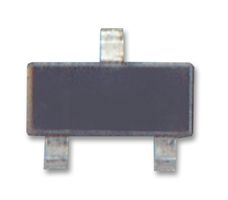
The FDN337N from Fairchild is N channel logic level enhancement mode power field effect transistor in superSOT-3 package. This transistor is produced using Fairchild»s proprietary, high cell density, DMOS technology, very high density process is especially tailored to minimize on state resistance, thus suite for low voltage applications in notebook computers, portable phones, PCMCIA cards and other battery powered circuits where fast switching and low inline power loss are needed in a very small outline surface mount package. . High density cell design for extremely low Rds(on) . Exceptional on resistance and maximum DC current capability . Drain to source voltage (Vds) of 30V . Gate to source voltage of ±8V . Low on state resistance of 65mohm at Vgs 4.5V . Continuous drain current of 2.2A . Maximum power dissipation of 500mW . Operating junction temperature range from -55°C to 150°C
FDN337N
Оплата онлайн или безналичный расчет 
FDN337N характеристики
МОП-транзистор, N Канал, 2.2 А, 30 В, 65 мОм, 4.5 В, 700 мВ.
The FDN337N from Fairchild is N channel logic level enhancement mode power field effect transistor in superSOT-3 package. This transistor is produced using Fairchild's proprietary, high cell density, DMOS technology, very high density process is especially tailored to minimize on state resistance, thus suite for low voltage applications in notebook computers, portable phones, PCMCIA cards and other battery powered circuits where fast switching and low inline power loss are needed in a very small outline surface mount package.
Техническое описание
Вы можете купить FDN337N от 1 штуки. Работаем с частными лицами и с юридическими лицами по безналичному расчету.
Доступно на складе 5520 штук. Цена FDN337N зависит от объёма заказа, минимальная стоимость составляет 35.2 руб.
FDN337N аналог FDN337N_NL и RTR040N03TL
The FDN337N from Fairchild is N channel logic level enhancement mode power field effect transistor in superSOT-3 package. This transistor is produced using Fairchild»s proprietary, high cell density, DMOS technology, very high density process is especially tailored to minimize on state resistance, thus suite for low voltage applications in notebook computers, portable phones, PCMCIA cards and other battery powered circuits where fast switching and low inline power loss are needed in a very small outline surface mount package. . High density cell design for extremely low Rds(on) . Exceptional on resistance and maximum DC current capability . Drain to source voltage (Vds) of 30V . Gate to source voltage of ±8V . Low on state resistance of 65mohm at Vgs 4.5V . Continuous drain current of 2.2A . Maximum power dissipation of 500mW . Operating junction temperature range from -55°C to 150°C
RTR040N03TL Обзор
The RTR040N03TL is a N-channel middle Power MOSFET offers 30V drain source voltage and ±4A continuous drain current. It is suitable for use in switching applications. . Low ON-resistance . Built-in G-S protection diode . Small surface-mount package . -55 to 150°C Operating junction temperature range
FDN337N
Оплата онлайн или безналичный расчет
FDN337N характеристики
МОП-транзистор, N Канал, 2.2 А, 30 В, 65 мОм, 4.5 В, 700 мВ.
The FDN337N from Fairchild is N channel logic level enhancement mode power field effect transistor in superSOT-3 package. This transistor is produced using Fairchild's proprietary, high cell density, DMOS technology, very high density process is especially tailored to minimize on state resistance, thus suite for low voltage applications in notebook computers, portable phones, PCMCIA cards and other battery powered circuits where fast switching and low inline power loss are needed in a very small outline surface mount package.
Техническое описание
Вы можете купить FDN337N от 1 штуки. Работаем с частными лицами и с юридическими лицами по безналичному расчету.
Доступно на складе 1935 штук. Цена FDN337N зависит от объёма заказа, минимальная стоимость составляет 54.16 руб.