Как выбрать mosfet.
1. Для начала надо узнать напряжение цепи в которой будет работать транзистор, это напряжение будет приложено к выводам Drain и Source.
Далее, необходимо отобрать транзисторы параметр Vds(Drain to Source Voltage ) которых минимум в 1.5 — 2 раза выше.
2. Другой не менее важный параметр — это ток, который мы хотим пропустить через транзистор. Максимальное значение тока, который можно пропустить через mosfet определяет параметр Id(Drain Current). Его значение также должно превышать реальный ток в 1.5 — 2 раза. Но это ещё не все, Id, в свою очередь, зависит от температуры.
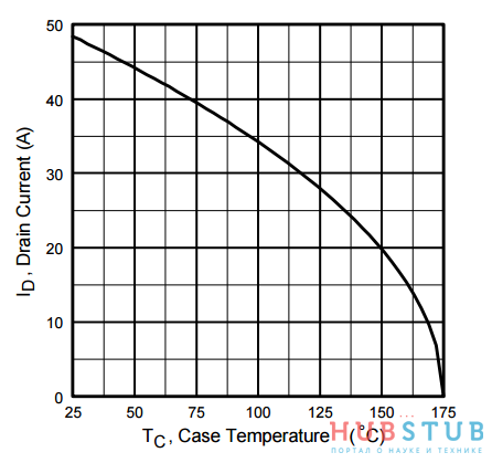
На графике видно, что с увеличением температуры корпуса ток, который может пропустить через себя транзистор уменьшается. Поэтому реальное значение Id надо выбирать исходя из того, при какой температуре mosfet будет работать.
3.Так как мы собираемся управлять нагрузкой, у нас наверняка должна быть управляющая схема и нам необходимо узнать какое напряжение у неё на выходе. Это напряжение подаётся на вывод, именуемый затвором или gate.
Напряжение на затворе транзистора ограничивают два параметра:
- Vgs(th)(Gate to Source Threshold Voltage) – пороговое напряжение затвор-исток при котором начинает открываться переход сток-исток
- Vgs(Gate to Source Threshold Voltage) — максимальное напряжение затвор-исток
- Rds(on) — Drain to Source On Resistance — сопротивление перехода сток-исток в открытом состоянии
- Rds(on) @ 10 V = 2.5 Ohms
- Rds(on) @ 4.5 V = 3 Ohms
Зная Rds можно найти ток, который потечёт через транзистор, для этого надо к сопротивлению нагрузки прибавить значение Rds и напряжение цепи поделить на получившееся сопротивление.
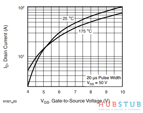
На этом графике представлена зависимость максимального Id от Vgs, если получившееся при расчётах значение меньше полученного из графика, идём дальше, если нет — ищем способ увеличить напряжение Vgs или другой транзистор.
5.Осталось только разобраться какая мощность будет выделяться на кристалле и способен ли эту мощность рассеять транзистор. И здесь есть один нюанс, обычно в даташите указывают максимальную мощность кристалла при температуре корпуса 25°
Что такое нижний RDS (on) МОП-транзистор?»
моя материнская плата Gigabyte GA-MA790XT-UD4P продается с Lower RDS(on) MOSFET . Мне любопытно, что это на самом деле значит.


13.12.2022 4:59 2869

1 ответ
Rds (ds должен быть подстрочным) означает » сопротивление (сток-к-источнику)», сток, где ток идет и источник, откуда он исходит.
МОП-транзисторы обычно используются в качестве лучшей альтернативы силовым транзисторам и используются для коммутации высокого тока.
имея более низкий Rds в основном означает, что меньше энергии будет потеряно через МОП-транзистор в соответствии с законом ом и, говоря, что их МОП-транзистор с низким Rds они в основном говорят, что их советы являются более энергоэффективными и, следовательно, будет производить немного меньше тепла в качестве побочного продукта MOSFET-транзистора.
Rds (on) в основном просто говорит, что Rds низкий, когда МОП-транзистор находится в состоянии «on». В выключенном состоянии транзистор не будет проводить, так что вы не заботитесь о сопротивлении.
маленькая деталь.
В простейшем использовать транзистор (или металл-оксид-полупроводник полевой транзистор) используется в качестве прямой замены для силовые транзисторы и реле. Символ для МОП-транзистора несколько похож на транзистор, но имеет зазор, иллюстрирующий тот факт, что нет прямой связи между затвором и другими частями транзистора, следовательно эффект поля транзистор.
Mosfet:  транзистор:
должный к факту что строб эффектно изолирован от настоящего путя (источника, котор нужно стечь) прибора это делает его много более полезно для более высоких токов, так как там гораздо меньше утечки через врата, тем самым увеличивая КПД устройства значительно.
большим преимуществом МОП-транзисторов для цифрового переключения заключается в том, что слой окисла между затвором и каналом предотвращает постоянный ток течет через ворота, дальнейшее снижение энергопотребления и давая очень большое входное сопротивление. Изолирующего оксида между затвором и канал эффективно изолирует МОП-транзистор в одном логическом каскаде от более ранних и более поздних стадий, что позволяет одному выходу МОП-транзистора управлять значительным количеством входов МОП-транзистора. Биполярная транзисторная логика (например, TTL) не обладает такой высокой разветвительной способностью.
из-за строительства на MOSFET существует еще сопротивление между истоком и стоком, даже когда полностью активированный (насыщенные) и это сопротивление вызывает некоторые тока через прибор, котор нужно расточительствовать и таким образом произвести жару. Уменьшение этого сопротивления уменьшает потери мощности и так же уменьшает количество тепла МОП.
по сравнению с транзистором МОП-транзистора высокоэффективный, с низким RDS и MOSFET является повышение эффективности власти.
Metal Oxide Field Effect Transistor: What is RDS(on)?
RDS(on) stands for “drain-source on resistance,” or the total resistance between the drain and source in a Metal Oxide Field Effect Transistor, or MOSFET when the MOSFET is “on.” RDS(on) is the basis for a maximum current rating of the MOSFET and is also associated with current loss. All things being equal, the lower the RDS(on), the better.
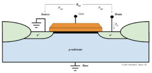 The voltage applied to the Gate determines if current will flow between the Source and Drain terminals. ID is the continuous drain current. (Image Credit: Kenneth Reese, III).
MOSFETs make perfect switching devices and are often used in power applications. Example applications for power MOSFETs include Switched Mode Power Supplies (SMPS), motor control, automotive, and in any application where a heavy-duty electronic switch is needed, such as a driver. Current flows between the n-channels when a gate-to-source voltage (VGS) is applied, otherwise the MOSFET behaves like a resistor. When VGS reaches the threshold voltage VGS(th), an inversion layer forms that enables current flow. The inversion layer becomes the conductive path (or channel) of the MOSFET between drain and source.
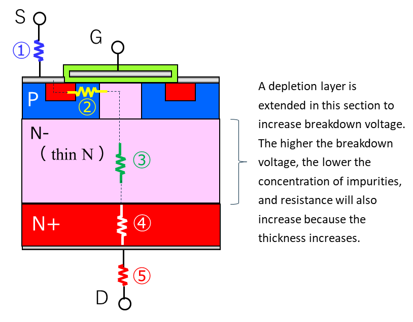
RDS(on), the total resistance in the path from source to drain, is made up of a series of resistances that traverses the path of current flow. RN is the source region’s diffusion resistance. RCH is the channel region’s resistance. RA is the resistance of an area called the accumulation region. RJ is the resistance of an area called the JFET region. RD is the drift region resistance and the most important factor in high-voltage MOSFETs. RS is the resistance of the substrate itself and can be ignored in high-voltage MOSFETs. However, in low voltage MOSFETs it can have a large effect on RDS(on). See Figure 2 of a vertical structure of a MOSFET and a series of resistances in series forms the total RDS(on) in the path of current flow from source to drain.
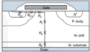 A MOSFET vertical structure, showing the total resistances that make up RDS(on). (Source: AN-9010 MOSFET Basics by ON Semi)
Besides these inherent structural contributors to RDS(on), imperfect contact between the source and drain metal and even the wiring that connects the die to the leads on the package can also contribute to RDS(on).[i] The latter can be identified as RWCML, or the total of the bond wire resistance, contact resistance, and the resistance of the lead frame.[ii]
RDS(on) increases with increasing temperature (this is also known as a positive temperature coefficient.) This is because of the mobility of the hole and electron decrease with increasing temperature.
RDS(on) is a function of temperature as defined by the following formula:
RDS(on) (T) = RDS(on) x (25°C) x (T/300) 2.3 , where T is absolute temperature.[i]
[i] AN-9010 MOSFET Basics. (2000). ON Semi Application Note, 1-17. Retrieved April 30, 2017.
[ii] IDAN0061 Power MOSFET Basics. Abdus Sattar, IXYS Corp. Retrieved April 30, 2017.
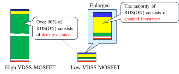
MOSFET ON resistance
This is a comparison of the RDS(ON) of a low VDSS MOSFET and
high VDSS MOSFET using the same package.
The size of the bare dies is nearly the same, but there is this much of a difference in RDS(ON).
Diode characteristic examples (Reference)
(Shindengen Electric Manufacturing Co., Ltd. products)
D1F60A (General Di)
Diode VF does not rely on VRRM as much as MOSFET RDS(ON).
What is ON resistance?
ON resistance (RDS (ON)) refers to the resistance from the D terminal to the S terminal which includes the channel resistance as well as other N layer resistance and wire and lead frame resistance, etc.
- Wire and lead frame resistance from the S terminal to the S electrode
- Channel resistance
- Drift resistance
- Silicon substrate resistance
- Solder and lead frame resistance from the electrode on the back of the bare die to the D terminal
RDS(ON) details
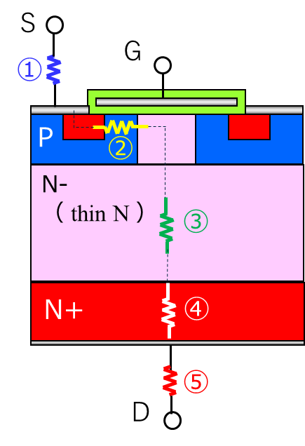
- Wire and lead frame resistance from the S terminal to the S electrode
- Channel resistance
- Drift resistance
⇒This varies greatly between high and low VDSS - Silicon substrate resistance
- Solder and lead frame resistance from the back of the bare die to the D terminal
Differences in drift layer between high and low VDSS MOSFETs
If voltage is applied between D-S, a depletion layer will extend to the N-layer based on the voltage.
The MOSFET VDSS is determined by the size (thickness) of the depletion layer on the N-layer.
High VDSS MOSFET
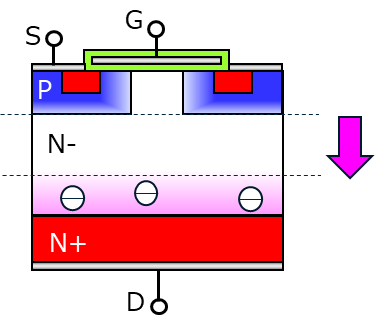
Low VDSS MOSFET
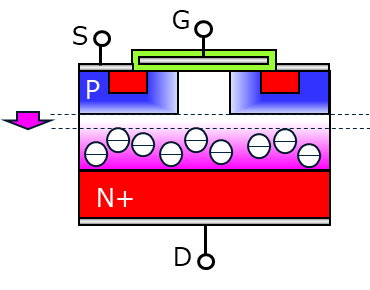
The MOSFET is designed so that the depletion layer can expand easily, so the N-layer (drift layer) is thick, and the impurity concentration is low.
⇒Resistance value is high when wanting to pass current through
The depletion layer only needs to extend a slight amount, so the N-layer (drift layer) is thin and the impurity concentration is high.
⇒Resistance value is low when wanting to pass current through
From this you can see that there is a “minimum resistance value” based on the required VDSS.
In order to lower RDS(ON)
- Manufacture a single bare die with a large number of clustered cells
⇒This is the basic methodology, however concentrating a large number of clustered cells will increase the bare die size and also increase the cost. - Make each cell as small as possible
⇒If channel length is shortened, the channel resistance per each individual cell will decrease, allowing for a higher concentration of cells on the same bare die area. - Utilize cell layout orientation
⇒This is what the trench technique consists of. Requires specialized processing for etching trenches. - Lower the resistance of components other than the channel
⇒A variety of techniques are utilized to lower resistance including lowering the resistance of the drift layer which increases VDSS, using connectors instead of wires, increasing lead frame and terminal thickness, etc.
Major technologies for lowering RDS(ON)
Degree of effectiveness
Details and aims
Low withstand voltage MOSFETs
High withstand voltage MOSFETs
The fundamental semiconductor processing technique. Equipment capacity.
Reduces channel resistance and miniaturizes cells.
Technology where trenches are etches and gates are embedded.
The main technique for low VDSS MOSFETs. Increases cell density.
Metallic conductors are used for connections instead of wires.
Lowers not only resistance, but also inductance.
PN stripe structures are created on the drift layer.
Lowers RDS(ON) below previous theoretical limitations.
Introduction of new materials such as SiC and GaN.
Allows for characteristics which were not achievable with Si.
Super Junction and Wide Band Gap are technologies for lowering drift layer resistance which are used in high VDSS MOSFETs.
Effects of RDS(ON) and capacitive components on circuit characteristics
Large bare die size
Ron — Low
Capacity — High
Price — High
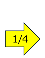
Small bare die size
Ron — High (4 times)
Capacity — Low (1/4)
Price — Low
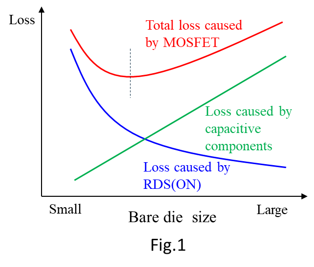
The larger the bare die size, the smaller the RDS(ON) will be, however capacity will also increase by the same amount, so there will be high power loss from switching, drive, etc.
If cost is ignored, the dashed line in the Fig.1 is the optimal performance. Simply having the lowest RDS(ON) is not optimal.